PIC microcontroller blinking LED without cheating
Table of Contents
1 Description
We configure a PIC microcontroller and design a blinking LED program, using just the data sheet and a text editor to build the hex file. We then start cheating by using tools to write the hex file to the PIC (it would be cool to do this step without cheating, meaning without using a programmer or anything else with a microcontroller).
This page explain:
- The behind-the-scenes low-level stuff related to programming microcontrollers.
- How delay functions work.
- How assemblers work.
- How Intel hex files work.
- How to set up input/output pins on a PIC.
- How the PIC is configured.
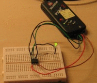
Figure 1: A gif is good enough
2 News
- 19 Sep. 2012: This page was featured on hackaday.com: Programming without a toolchain; crafting PIC op code by hand. There are a lot of great comments about manual assembling in the good old days.
- 16 Sep. 2012: Initial page.
3 The PIC
We use the PIC12F1840. It is a mid-range model with 8 pins. We refer to the PIC12F1840 data sheet as 12f1840sheet.
4 Device configuration
The PIC can be configured by setting bits in two configuration words (PIC words are 14 bits wide) on the PICs flash memory.
These configuration words are located at word 0x8007 (configuration word 1) and 0x8008 (configuration word 2) (12f1840sheet p. 41).
The default options are 1s for all bits in the configuration words. The changes we describe use different values than the defaults.
4.1 Which options we need to set
- Enable internal oscillator
- Disable low-voltage programming and pin reset (to get an extra input pin)
- Set internal oscillator to 32 MHz
4.2 Use Internal Oscillator
To enable the internal oscillator we need to set bits 0-2 of
configuration word 1 to 100 (12f1840sheet p. 43).
Since the default configuration bits are 1s, our configuration word 1 now looks like:
0x8007: 11 1111 1111 1100
4.3 Disable low-voltage programming and pin reset
To disable low-voltage programming we set bit 13 of configuration word 2 to 0 (12f1840sheet p.44). We also need to set bit 6 of configuration word 1 to 0 in order to define pin 4 as an digital input (instead of a reset pin). Remembering our changes from the previous section our configuration words looks like:
0x8007: 11 1111 1011 1100
0x8008: 01 1111 1111 1111
4.4 Set internal oscillator to 32 MHz
By default the internal oscillator runs at 500 kHz. We can change the clock frequency by changing the OSCCON internal memory register (12f1840sheet p. 54).
To set the oscillator to 32 MHz the value of OSCCON should be 1111
0000 (12f1840sheet p. 61). The location of OSCCON is 0x19 in page
bank 1 (12f1840sheet p. 20).
To set up OSCCON with the correct value we need a sequence of instructions (12f1840sheet p. 309):
movlw 0xF0 ; store OSCCON value (1111 0000) in W
movlb 0x01 ; Select page bank 1
movwf 0x19 ; move value of W to register at OSCCON (address 0x19)
The instruction movlw 0xF0 (move literal to W) sets the value of
the W register to the argument (0xF0) (12f1840sheet p. 316).
The instruction movlb 0x01 (move literal to b) sets b (the
currently active internal memory page bank) to the argument (0x01)
(12f1840sheet p. 316).
The instruction movwf 0x19 (move W to f) copies the values of
W to the register whose address matches the argument (0x19)
(12f1840sheet p. 316).
5 Blinking LED program
The Blinking LED program blinks a LED connected to an output pin of the PIC to be on for a second, then off for a second, and repeats this sequence.
5.1 Setting up an output pin
We use pin 5 (RA2) as the output. To initialize output and define RA2
as an output pin we first clear the registers PORTA, LATA and ANSELA,
then we set bit 2 of TRISA to 1 (12f1840sheet p. 113). The internal
memory addresses of these registers are all 0x0C but they are in
different data banks: PORTA is in bank 0, LATA is in bank 2, ANSELA is
in bank 3 and TRISA is in bank 1 (12f1840sheet p. 20).
The following instructions sets up RA2 as an output port (12f1840sheet p.113):
movlb 0     ; select bank 0 (PORTA)
clrf 0x0C   ; clear PORTA

movlb 2     ; select bank 2 (LATA)
clrf 0x0C   ; clear LATA

movlb 3     ; select bank 3 (ANSELA)
clrf 0x0C   ; clear ANSELA

movlb 1     ; select bank 1 (TRISA)
bcf 0x0C, 2 ; define RA2 as an output port (clear TRISA bit 2)
The instruction clrf 0x0C (clear f) sets the value of 0x00 to the
register whose address matches the argument (0x0C) (12f1840 p. 313).
The instruction bcf 0x0C, 2 (bit clear f) sets the bit matching the
second argument to 0 in the register whose address match the first
argument (0x0C) (12f1840 p. 312).
5.2 Changing the output
To change the output of the pin (RA2, pin 5), we set bit 2 in the internal memory register PORTA (12f1840sheet p. 113).
To light up the LED we set the output pin to 1:
movlb 0     ; select bank 0 (PORTA)
bsf 0x0C, 2 ; set the 2nd bit of PORTA (address 0x0C) to 1
The instruction bsf 0x0C, 2 (bit set f) sets the bit matching the
second argument (2) to 1 in the register whose address match the first
argument (0x0C) (12f1840 p. 312).
To turn off the LED we set the output pin to 0:
movlb 0     ; select bank 0 (PORTA)
bcf 0x0C, 2 ; set the 2nd bit of PORTA (address 0x0C) to 0
5.3 Waiting for 1 second
To have the PIC wait for 1 second we give it a bunch of instructions to do.
We have set the PIC's oscillator to run at 32 MHz. The PIC uses 4 oscillator cycles to execute 1 instruction cycle (12f1840sheet p. 307). Each second the PIC executes 8,000,000 instruction cycles.
5.3.1 Wait-1-second program
We wait a second by designing a program that takes 8,000,000 instruction cycles to execute.
We design this program as a series of nested loops. To make loops we
need variables. The PIC have general purpose registers we can use as
variables beginning from the internal memory address 0x20 in data
banks 0-2 (12f1840 p. 20). We use the three registers 0x20, 0x21
and 0x22. Each register holds 1 byte (values from 0 to 255).
Our wait-1-second program:
movlw 0x43     ; 0x43 = 67
movwf 0x20     ; set 0x20 to 67
movlw 0xC7     ; 0xC7 = 199
movwf 0x21     ; set 0x21 to 199
movwf 0x22     ; set 0x22 to 199
decfsz 0x22, 1 ; decrement 0x22
bra $-1        ; if 0x22 != 0 go back 1 instruction
decfsz 0x21, 1 ; decrement 0x21
bra $-4        ; if 0x21 != 0 go back 4 instruction
decfsz 0x20, 1 ; decrement 0x20
bra $-7        ; if 0x20 != 0 go back 7 instructions
The instruction decfsz 0x22, 1 (decrement f, skip if 0) does 3
things (12f1840sheet p. 314):
- Decrements the register whose address matches the first argument
(
0x22); - If the second argument is 0, save the decremented value to W, if the second argument is 1, save the decremented value back to itself; And
- Skips the next instruction if the decremented value is 0.
The instruction bra $-1 (relative branch) is a relative goto. It
jumps forward or backward the amount of instructions specified in the
argument. $-1 executes the instruction before the bra, an argument
of $0 would go to itself. However, bra adds k + 1 to the PC
(program counter) (12f1840 p. 312), which means that bra $-1 should
jump to itself. Assemblers use the first notation (bra $-1 jumps to
the previous instruction), but outputs code as if the instruction was
bra $-2. We use the same notation as the assemblers (bra $-1 jumps
to the previous instruction).
This program takes 8,000,003 instructions to execute. The program consists of 3 nested for loops. Writing the program in C, while preserving the order of the instructions, would look like:
unsigned char _0x20, _0x21, _0x20;
            /* movlw 0x43 */
_0x20 = 67; /* movwf 0x20 */
            /* movlw 0xC7 */
do {
  _0x21 = 199; /* movwf 0x21 */

  do {
    _0x22 = 199; /* movwf 0x22 */

    while (_0x22-- != 0) { } /* decfsz 0x22, 1 */
                             /* bra $-1 */

  } while (_0x21-- != 0); /* decfsz 0x21, 1 /*
                          /* bra $-4 */

} while (_0x20-- != 0); /* decfsz 0x20, 1 */
                        /* bra $-7 */
A more C-friendly approach would look like:
#+BEGIN_SRC c unsigned char _0x20, _0x21, _0x20; for (_0x20 = 67; _0x20 != 0; _0x20–) { for (_0x21 = 199; _0x21 != 0; _0x21–) { for (_0x22 = 199; _0x22 != 0; _0x22–) { * do nothing * } } } #+END_SRC c
5.3.2 Why the wait-1-second program works
The wait-1-second program works because it takes 8,000,000 instruction cycles to execute. We now verify this by examining the program.
5.3.2.1 0x22 loop (inner-most)
Let us start with the inner-most loop:
decfsz 0x22, 1 ; decrement 0x22
bra $-1        ; if 0x22 != 0 go back 1 instruction
The decfsz instruction use 1 instruction cycle if 0x22 is not 0,
and 2 cycles if 0x22 is 0.
The bra instruction always use 2 instruction cycles.
As 0x22 is initialized to 198 we get (1 + 2) * 198 + 2 = 596 instruction
cycles.
- The 1 is from
decfsz, - the first 2 is from
bra, - the 198 is the number of times
0x22is not 0, and - the last 2 is from
decfszwhen0x22is 0 (when0x22is 0 thebrainstruction is skipped).
This equation can also be written as (1 + 2) * 199 - 1 = 596.
5.3.2.2 0x21 loop
The rest of the loops work the same as the inner-most, let us look at
the 0x21 loop.
movwf 0x22     ; set 0x22 to 199
...            ; 0x22 loop
decfsz 0x21, 1 ; decrement 0x21
bra $-4        ; if 0x21 != 0 go back 4 instruction
As 0x21 is initialized to 199 we get (1 + 596 + 1 + 2) *
199 - 1 = 119399.
- The first 1 is from
movwf 0x22, - the 596 is the number of instruction cycles from the
0x22loop, - the 1 is from
decfsz, - the 2 is from
bra, - the 199 is the number of times the loop is executed, and
- the -1 accounts for the case where
0x21is 0.
5.3.2.3 0x20 loop (outer-most)
movwf 0x21     ; set 0x21 to 199
...            ; 0x21 loop
decfsz 0x20, 1 ; decrement 0x20
bra $-7        ; if 0x20 != 0 go back 7 instructions
As 0x20 is initialized to 67 we get (1 + 119399 + 1 + 2) *
67 - 1 = 8000000.
5.3.2.4 The full loop
Now we just need to account for our initialization code.
movlw 0x43     ; 0x43 = 67
movwf 0x20     ; set 0x20 to 67
movlw 0xC7     ; 0xC7 = 199
...            ; 0x20 loop
As movlw and movwf both use 1 instruction cycle, we get 3 +
8000000 = 8000003.
So our wait-1-second program takes 8,000,003 instructions to execute, at 8 MHz this takes 1.000000375 seconds.
5.4 Putting the blinking LED program together
We now have all we need to put out blinking LED program together. An assembly version of this program can also be downloaded: blinkled.asm.
;;; Set internal oscillator to 32 MHz
movlw 0xF0 ; store OSCCON value (=1111 0000=) in W
movlb 0x01 ; Select page bank 1
movwf 0x19 ; move value of W to register at OSCCON (address 0x19)

;;; Define pin 5 (RA2) as output
movlb 0     ; select bank 0 (PORTA)
clrf 0x0C   ; clear PORTA

movlb 2     ; select bank 2 (LATA)
clrf 0x0C   ; clear LATA

movlb 3     ; select bank 3 (ANSELA)
clrf 0x0C   ; clear ANSELA

movlb 1     ; select bank 1 (TRISA)
bcf 0x0C, 2 ; define RA2 as an output port (clear TRISA bit 2)

;;; Turn on LED (set pin 5 to 1)
movlb 0     ; select bank 0 (PORTA)
bsf 0x0C, 2 ; set the 2nd bit of PORTA (address 0x0C) to 1

;;; Wait 1 second
movlw 0x43     ; 0x43 = 67
movwf 0x20     ; set 0x20 to 67
movlw 0xC7     ; 0xC7 = 199
movwf 0x21     ; set 0x21 to 199
movwf 0x22     ; set 0x22 to 199
decfsz 0x22, 1 ; decrement 0x22
bra $-1        ; if 0x22 != 0 go back 1 instruction
decfsz 0x21, 1 ; decrement 0x21
bra $-4        ; if 0x21 != 0 go back 4 instruction
decfsz 0x20, 1 ; decrement 0x20
bra $-7        ; if 0x20 != 0 go back 7 instructions

;;; Turn off LED (set pin 5 to 1)
bcf 0x0C, 2 ; set the 2nd bit of PORTA (address 0x0C) to 1

;;; Wait 1 second
movlw 0x43     ; 0x43 = 67
movwf 0x20     ; set 0x20 to 67
movlw 0xC7     ; 0xC7 = 199
movwf 0x21     ; set 0x21 to 199
movwf 0x22     ; set 0x22 to 199
decfsz 0x22, 1 ; decrement 0x22
bra $-1        ; if 0x22 != 0 go back 1 instruction
decfsz 0x21, 1 ; decrement 0x21
bra $-4        ; if 0x21 != 0 go back 4 instruction
decfsz 0x20, 1 ; decrement 0x20
bra $-7        ; if 0x20 != 0 go back 7 instructions

;;; Loop
bra $-24
The last instruction loops back to where the LED is turned on.
6 Building the hex file
Hex files use the Intel Hex 32-bit format. Hex files consist of data, information about where the information should be placed and checksums to protect against corrupted. Hex files consists of lines containing an address, some data, a checksum, and other things, these lines are called records. Special records can represent the end of the hex file or use bigger addresses than the regular data record can represent.
Our program consist of two sets of data: the configuration words and the program itself.
6.1 The configuration words
From the previous section (Device configuration), our configuration words are:
0x8007: 11 1111 1011 1100
0x8008: 01 1111 1111 1111
However, this data need to be changed to hex file format. We need to change (1) pad to 8-bit boundary, (2) the addressing, (3) the endian and (4) the value representation.
- The hex file understands bytes. PIC words, however, are 14 bits wide, so we need to pad them to have their lengths be a multiply of 8. We add two 1's to the left of our configuration words to solve this.
- Our addresses (0x8007 and 0x8008) point to words (14 bits words padded to 16 bits), but addresses in hex files point to bytes. We solve this difference by simply doubling the addresses, getting us 0x1000E and 0x10010.
- We have written the bytes of the configuration words as big-endian
byte order (the most-significant byte is first), but hex files use
little-endian byte order. We solve this difference by swapping the
two bytes of each of our configuration words so
0001 0010 0100
   1000
would become0100 1000 0001 0010. - We represent the values of the configuration words in binary, but hex files represent values in hexadecimal. We solve this difference by converting to hexadecimal.
Applying these changes give us a new representation of our configuration words:
0x1000E: BC FF
0x10010: FF DF
To represent our configuration words in the hex file we first give the address and then the data.
To set the address we need a special record as the address is too big (bigger than what is addressable using 16 bits). This special record sets the most-significant 16 bits of a 32-bit address. These most-significant 16 bits are added to the 16-bit addresses of regular records in the hex file to get a 32-bit address. This record consist of:
:The start code for every record in a hex file.02The number of bytes of data represented in this record. Our record define the most-significant 16 bits or 2 bytes of future addresses.0000The least-significant 16-bits of the address. In this type of record, this field is not meaningful.04The type of record. Type04is the extended linear address record.0001The data of the record. The1is the first1in our configuration words addresss (0x1000E, or written as a 32-bit address:0x0001000E).F9The checksum. This is the least-significant byte of the sum of the bytes of previous fields subtracted from 0x100. This gives us:
0x100 - ((0x02 + 0x0000 + 0x04 + 0x0001) % 256) =
256 - ((2 + 4 + 1) % 256) =
249 = 0xF9
Now we can add the record containing the values of the configuration words. For this we use a regular data record:
:Start code.04The number of bytes. We have 2 configuration words, each consisting of 2 bytes.000EThe address. Combining these least-significant 16 bits with the most-significant 16 bits from the previous record gives us0x1000E, which is the address of the first configuration word.00The type of record. Type00is a data record.BCFFFFDFThe data. This is the values of the configuration words. Since the configuration words is next to each other in memory, we can combine them into a single record in the hex file.55The checksum:
0x100 - ((0x04 + 0x00 + 0x0E + 0x00 + 0xBC + 0xFF + 0xFF + 0xDF) % 256) =
256 - ((4 + 14 + 188 + 255 + 255 + 223) % 256) =
85 = 0x55.
The two hex records for setting the configuration words are:
:020000040001F9
:04000E00BCFFFFDF55
6.2 The program
To convert our blinked LED program to hex file format, we first have to translate the instructions to their binary opcodes, and then change our data to be in the same format as hex files.
6.2.1 Translating instructions to binary opcodes
A binary opcode is the sequence of bits that tell the PIC what instruction it is executing as well as the argument of the instruction (12f1840sheet p. 309-310).
Let us translate the instruction movlw 0xF0. The instruction movlw
has the opcode 11 0000 kkkk kkkk where k is the argument. The
argument 0xF0 is 1111 0000. Combining these give the final binary
opcode as 11 0000 1111 0000 (12f1840sheet p. 309).
The instruction bsf 0x0C, 2 follows the same principle but have two
arguments. bsf have the opcode 01 01bb bfff ffff. The first
argument 0x0C is 0000 1100. The second argument 2 is 0000
0010. If we combine the 7 least-significant bits of the first
argument, the 3 least-significant bits of the second and the opcode,
we get 01 0101 0000 0011.
The instruction bra $-7 has a negative number. bra has the opcode
11 001k kkkk kkkk. As mentioned earlier, when we write bra $-7, we
actually mean bra $-8, so the true argument is -8. -8 is a
negative number, we represent negative numbers in binary using
two-complement. One method of finding the binary representation of a
negative number is to take the positive representation (0000 1000),
invert all the bits (1111 0111) and add 1 (1111 1000). In the
bra opcode the argument consist of 9 bits. To pad a negative number
we add 1s to the left of the number (-8 = 1111 1000 = 1 1111
1000). When we combine our opcode and argument we get 11 0011 1111
1000.
Translating all instructions give us:
11 0000 1111 0000   movlw 0xF0
00 0000 0010 0001   movlb 0x01
00 0000 1001 1001   movwf 0x19

00 0000 0010 0000   movlb 0
00 0001 1000 1100   clrf 0x0C

00 0000 0010 0010   movlb 2
00 0001 1000 1100   clrf 0x0C

00 0000 0010 0011   movlb 3
00 0001 1000 1100   clrf 0x0C

00 0000 0010 0001   movlb 1
01 0001 0000 1100   bcf 0x0C, 2

00 0000 0010 0000   movlb 0
01 0101 0000 1100   bsf 0x0C, 2

11 0000 0100 0011   movlw 0x43
00 0000 1010 0000   movwf 0x20
11 0000 1100 0111   movlw 0xC7
00 0000 1010 0001   movwf 0x21
00 0000 1010 0010   movwf 0x22
00 1011 1010 0010   decfsz 0x22, 1
11 0011 1111 1110   bra $-1
00 1011 1010 0001   decfsz 0x21, 1
11 0011 1111 1011   bra $-4
11 1011 1010 0000   decfsz 0x20, 1
11 0011 1111 1000   bra $-7

01 0001 0000 1100   bcf 0x0C, 2

11 0000 0100 0011   movlw 0x43
00 0000 1010 0000   movwf 0x20
11 0000 1100 0111   movlw 0xC7
00 0000 1010 0001   movwf 0x21
00 0000 1010 0010   movwf 0x22
00 1011 1010 0010   decfsz 0x22, 1
11 0011 1111 1110   bra $-1
00 1011 1010 0001   decfsz 0x21, 1
11 0011 1111 1011   bra $-4
00 1011 1010 0000   decfsz 0x20, 1
11 0011 1111 1000   bra $-7

11 0011 1101 1101   bra $-24
Assemblers are useful.
6.2.2 Change opcodes to hex file format
To change our opcodes to hex file format we need to (1) pad to 8-bit boundary, (2) convert to hexadecimal, (3) change the byte endian and (4) consider where to put our program.
We have explained most of these changes in the previous section The configuration words.
We have to consider where to place the program inside the PICs flash
memory. There are two important positions in the flash memory: the
reset vector at word 0x0000 and the interrupt vector at word
0x0004 (12f1840sheet p. 15). The reset vector is where the PIC
starts executing instructions when powered on or after it has been
reset. The interrupt vector is where instructions are executed from
after an interrupt have been triggered. However, we do not care about
interrupts, so we are going to place our program at 0x0000, and past
the interrupt vector. This placement means an interrupt would cause
the PIC to start executing in the middle of our program and after 16
interrupts the PIC will run out of stack and reset (12f1840sheet
p. 35,44). We have not enabled interrupts, so this is not a problem.
Let us convert the instruction movlw 0xF0 to hex file format. The
instruction movlw 0xF0 has the binary opcode 11 0000 1111
0000. First we pad the opcode to be 16 bits wide, giving us 0011
0000 1111 0000. Second we convert to decimal giving us 30 F0. And
finally we swap the two bytes giving us F0 30. Repeating this
process for our whole program gives us:
swap    hex     binary opcode       instruction
==================================================
F0 30   30 F0   11 0000 1111 0000   movlw 0xF0
21 00   00 21   00 0000 0010 0001   movlb 0x01
99 00   00 99   00 0000 1001 1001   movwf 0x19

20 00   00 20   00 0000 0010 0000   movlb 0
8C 01   01 8C   00 0001 1000 1100   clrf 0x0C

22 00   00 22   00 0000 0010 0010   movlb 2
8C 01   01 8C   00 0001 1000 1100   clrf 0x0C

23 00   00 23   00 0000 0010 0011   movlb 3
8C 01   01 8C   00 0001 1000 1100   clrf 0x0C

21 00   00 21   00 0000 0010 0001   movlb 1
0C 11   11 0C   01 0001 0000 1100   bcf 0x0C, 2

20 00   00 20   00 0000 0010 0000   movlb 0
0C 15   15 0C   01 0101 0000 1100   bsf 0x0C, 2

43 30   30 43   11 0000 0100 0011   movlw 0x43
A0 00   00 A0   00 0000 1010 0000   movwf 0x20
C7 30   30 C7   11 0000 1100 0111   movlw 0xC7
A1 00   00 A1   00 0000 1010 0001   movwf 0x21
A2 00   00 A2   00 0000 1010 0010   movwf 0x22
A2 0B   0B A2   00 1011 1010 0010   decfsz 0x22, 1
FE 33   33 FE   11 0011 1111 1110   bra $-1
A1 0B   0B A1   00 1011 1010 0001   decfsz 0x21, 1
FB 33   33 FB   11 0011 1111 1011   bra $-4
A0 0B   0B A0   00 1011 1010 0000   decfsz 0x20, 1
F8 33   33 F8   11 0011 1111 1000   bra $-7

0C 11   11 0C   01 0001 0000 1100   bcf 0x0C, 2

43 30   30 43   11 0000 0100 0011   movlw 0x43
A0 00   00 A0   00 0000 1010 0000   movwf 0x20
C7 30   30 C7   11 0000 1100 0111   movlw 0xC7
A1 00   00 A1   00 0000 1010 0001   movwf 0x21
A2 00   00 A2   00 0000 1010 0010   movwf 0x22
A2 0B   0B A2   00 1011 1010 0010   decfsz 0x22, 1
FE 33   33 FE   11 0011 1111 1110   bra $-1
A1 0B   0B A1   00 1011 1010 0001   decfsz 0x21, 1
FB 33   33 FB   11 0011 1111 1011   bra $-4
A0 0B   0B A0   00 1011 1010 0000   decfsz 0x20, 1
F8 33   33 F8   11 0011 1111 1000   bra $-7

DB 33   33 DB   11 0011 1101 1011   bra $-24
This leave us with our translated program as a sequence of hexadecimal numbers:
F0 30 21 00 99 00 20 00 8C 01 22 00 8C 01 23 00
8C 01 21 00 0C 11 20 00 0C 15 43 30 A0 00 C7 30
A1 00 A2 00 A2 0B FE 33 A1 0B FB 33 A0 0B F8 33
0C 11 43 30 A0 00 C7 30 A1 00 A2 00 A2 0B FE 33
A1 0B FB 33 A0 0B F8 33 DB 33
To convert this sequence to hex file format we first set the address
to 0x0000, then split the data out over 5 data records.
From the previous section (6.1) we know how to set
the extended address. The checksum calculation is 256 - ((2 + 4)
% 256) = 250 = FA. This gives us the extended linear address record:
:020000040000FA
We have also seen how data records work from the same previous section. Our 5 data records are:
:10000000F0302100990020008C0122008C01230097
:100010008C0121000C1120000C154330A000C730CA
:10002000A100A200A20BFE33A10BFB33A00BF833FF
:100030000C114330A000C730A100A200A20BFE3378
:0A004000A10BFB33A00BF833DB33F8
Note that the data records have 16 = 0x10 bytes of data, and that
the address is increased by 0x10 = 16 bytes for each record. The
last data record has 10 (0x0A) bytes of data.
The checksum calculation for the first record is:
0x100 - ((0x10 + 0xF0 + 0x30 + 0x21 + 0x99 + 0x20 + 0x8C + 0x01 + 0x22
          + 0x8C + 0x01 + 0x23) % 256)
= 256 - (16 + 240 + 48 + 33 + 153 + 32 + 140 + 1 + 34 + 140 + 1 + 35) % 256
= 151 = 0x97
The other checksum calculations are equally boring and was left out.
To end the hex file we add a special end-of-file record. The
end-of-file record has record type 01, no data and a checksum of
0xFF:
:00000001FF
Finally, we put it all together to get our hex file blinkled.hex:
:020000040001F9
:04000E00BCFFFFDF55
:020000040000FA
:10000000F0302100990020008C0122008C01230097
:100010008C0121000C1120000C154330A000C730CA
:10002000A100A200A20BFE33A10BFB33A00BF833FF
:100030000C114330A000C730A100A200A20BFE3378
:0A004000A10BFB33A00BF833DB33F8
:00000001FF
7 Writing the program to the PIC (the cheating part)
Getting a hex file unto a PIC is preferable done using a pickit 3 and mplab_ipe. I, however, only have a pickit 2 (which isn't currently supporting the PIC12f1840), so I have to do some extra work.
7.1 Setting up pk2cmd
This section is mostly for my future self, do not be too upset if it does not for your system.
We need at least version 1.21, but the official pickit 2 site only has version 1.20 at the moment. However, a testing pk2cmd version 1.21 has been made available on the Microchip forums.
Beside pk2cmd, we also need a device file (version 1.62.14 works). This file is available from the official pickit 2 site.
To unpack, compile and install pk2cmd this sequence of commands worked for my Ubuntu 11.10 system:
unzip -d PICkit2_PK2CMD_WIN32_SourceV1-21_RC1 \
         PICkit2_PK2CMD_WIN32_SourceV1-21_RC1.zip
unzip -d PK2DFUpdate-1-62-14 PK2DFUpdate-1-62-14.zip

cd PICkit2_PK2CMD_WIN32_SourceV1-21_RC1
cd pk2cmd
cd pk2cmd
make linux
cp ../../../PK2DFUpdate-1-62-14/PK2DeviceFile.dat .
sudo make install

echo 'PATH=$PATH:/usr/share/pk2' | sudo tee --append /etc/profile
echo 'export PATH' | sudo tee --append /etc/profile
7.2 Uploading a hex file using pk2cmd
This is how I set up the PIC, the pickit2 and the LED (with a 1K resistor).

To test if everything is hooked up correctly we run:
pk2cmd -PPIC12F1840 -I
Next we upload the hex file and power the PIC through the pickit 2:
pk2cmd -PPIC12F1840 -Fblinked.hex -M -T
To just start powering the PIC through the pickit 2 we run:
pk2cmd -PPIC12F1840 -T